PCB Layout & Routing
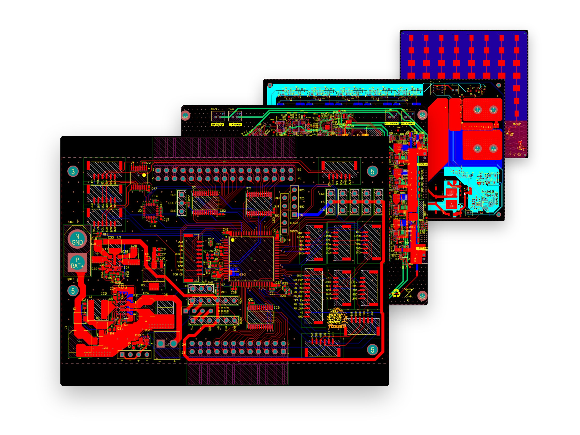
Turn your schematics into a manufacturing-ready PCB, with careful component placement, stack-up design and routing for electrical performance and reliable assembly.
64
layers max
100k+
pins routed
48 h
to kick-off
Workflow
Netlist in, Gerber out
01 · You provide
Design Inputs
SchematicsBoard outlineLibrariesRequirements
02 · We develop
Place & route
Stack-upPlacementRouting
03 · We review
Review & Refine
Design checksYour feedbackFinal approval
04 · You receive
Build package
Source filesFabricationAssemblyDrawings
Scope
PCB constructions & applications
R
Rigid
Multilayer boards with stack-ups suited to your electrical and mechanical requirements.
F
Flex
Flexible circuits with routing and bend regions planned around the assembly.
RF
Rigid-flex
Integrated rigid and flexible sections for compact, interconnected assemblies.
µ
HDI
Fine-pitch components, microvias and via-in-pad for dense PCB layouts.
GHz
High-speed
Controlled impedance, length matching and return-path planning.
kW
Power
High-current routing, copper sizing, thermal management and electrical clearances.
Capability sheet
Defined around your requirements
- EDA Software
- Kicad, Altium
- Kick-off after scope
- < 48 h
Deliverables
Files you get back
.PcbDoc
layout source
GBR X2
fabrication
ODB++
CAM data
BOM.xlsx
sourcing-ready
PNP.csv
pick & place
.pdf
assembly drawings
Source files included in Mode 1 engagements — talk through your scope.